Multilayer pcb manufacturing process pdf
Multilayer PCB Manufacturer –Hitechpcb specializing in multilayer pcb, multi-layer PCB, High density PCB, High Density Interconnect PCBs (HDI PCBs), quick turn pcb prototype in China.
Extra steps are required in the design and manufacturing process for testing advanced printed wiring boards (PWBs) with embedded passive components. This processing is further complicated by
The ‘Global and Southeast Asia High-Frequency Multilayer PCB Industry, 2013-2023 Market Research Report’ is a professional and in-depth study on the current state of the global High-Frequency Multilayer PCB industry with a focus on the Southeast Asia market.
This paper is in the process of Multilayer PCB laminate technology! Multilayer printed circuit board is composed of more than three layers of conductive graphics layer and insulation layer alternately by laminated gluing together and form of the PCB, and meet the design requirements stipulated conductive graphics interconnection between the layers. It has high density, small volume, light
The definition of multilayer PCB Copper foil layer is bonded together by PP(prepreg), Multilayer PCB is one of the most complex types in printed circuit board. Because of the complexity in PCB manufacturing process , low yield rate and difficulty of rework, making the price is relatively high.
The PCB manufacturing process is an essential element of the electronics production lifecycle. PCB manufacturing employs many new areas of technology and this has enabled significant improvements to be made both in the reduction of sizes of components and tracks used, and in …
Understanding The Multilayer PCB Fabrication Process A huge question for people interested in PCB’s (Printed Circuit Boards) are first, what are PCBs made of? The basis of most quality printed circuit boards use FR4, which is a rigid type of fiberglass laminate.
The manufacturing process. CAM editing The data records of the customer are converted into the Ext. Gerber format (RS 274X). The processed output file in the Extended Gerber Format can be supplied as preview if desired. A pre-production preview of the PCB layout can be supplied in PDF format. Order tracking. Material Preparation The copper-clad panels along with the drill entry material & a
The sequential lamination process in combination with thin film embedded resistors requires a different processing sequence than conventional multilayer manufacturing with thin film embedded resistors.
PCB Multi-layer Fabrication – Lay-up and Bond The outer layers of our multi-layer consist of sheets of glass cloth pre-impregnated with uncured epoxy resin (prepreg) and a thin copper foil. The lay-up operator has already placed a copper foil and 2 sheets of prepreg on the heavy steel baseplate.
In general, there are three types of Multilayer PCB: Single layer, double layer and multilayer PCB. There is not much difference in a single layer and double layer PCB. Single layer is having copper traces on one side and double layer PCB is having traces on both sides, both of …
Multilayer Printed Circuit Boards. Millennium Circuits Limited is a leading supplier of PCB multilayer boards, which are more complex and have a variety of differences from the standard single- …
the art PCB solution. The result was a new process with 69 layers, 11 The result was a new process with 69 layers, 11 sequential lamination steps and over 250,000 plated through holes.
Printed circuit boards manufacturing The board consists of resin, reinforcement, copper foil, and of course a lamination process. Although broadly similar to the manufacture of multilayer boards, the production of base laminate is generally carried out by specialists, who supply board fabrication houses with process blanks. ‘Rolling your . 2 own’ laminate is a possibility, but one that
To explain the PCB manufacturing process at Electronic Interconnect, we are including 3 flow charts that highlight the PCB process. The PCB fabrication process can be complex and confusing. Electronic Interconnect manufactures single-, double- and multilayer circuit boards.
To produce the inner layers of our multilayer PCB, we start with a panel of laminate. Laminate is an epoxy resin and glass-fibre core with copper foil pre-bonded onto each side. Laminate is an epoxy resin and glass-fibre core with copper foil pre-bonded onto each side.
The proposed system is designed using CST software and fabricated using conventional Printed Circuit Board (PCB) manufacturing process on Rogers 4003 C with = 3.38 and thickness of 0.813 mm. The
Designing a Multilayer PCB Stackup to Balance Signal Integrity Against Manufacturability and Reliability PRESENTED TO IEEE EMC GROUP SANTA CLARA, CA SEPTEMBER 13, 2011 LEE W. RITCHEY SPEEDING EDGE ©SPEEDING EDGE SEPTEMBER 2011. Speeding Edge, SPRING 2010 SLIDE # 2 THE CHANGING WORLD OF PCB FABRICATION • At the outset of PCB fabrication …
PCB Manufacturing Process Flow Chart – PCB Fabrication
https://www.youtube.com/embed/rLBChuikmGU

High-Frequency Multilayer PCB Market Report – Research
Welcome to get the customized multilayer pcb with our professional manufacturers and suppliers. Through strict manufacturing process, we can assure you of the high quality and high efficiency of our multilayer pcb. Please be free to contact our factory.
Multilayer PCB Prototype & Manufacture in ALLPCB.com. Unlike single-sided and double-sided PCB board, multilayer PCB board manufacturing has higher requirement on the manufacturing capability because all multilayer PCBs at least have three layers of …
PCBGOGO, a professional and trustworth PCB and PCBA manufacturer with over 10 years, highly specialized not only in quick-turn PCB prototype and PCB assembly,but also medium and small volume PCB …
Therefore, producing a PCB is a complex process of many steps. This overview covers the most important steps when producing a multilayer PCB. This overview covers the most important steps when producing a multilayer PCB.
DESCRIPTION. Flowchart of multilayer bare printed circuit board fabrication process. Flow chart available in poster format.
which hardens when heated and pressed during the PCB fabrication process. Isola’s FR406 materials – include 1.7, 2.3, 3.9 and 7.1 MIL prepregs that may be combined to achieve the desired prepreg thickness. The most common stackup called the ‘Foil Method’ is to have prepreg with copper foils bonded to the outside on the outer most layers (top and bottom) then core alternating with
Multilayer PCB Why stack-up? With the development of electronic products, PCBs are facing more requirements including miniaturization, low weight, high speed and capacity and multiple functions, which results in the popularity of multilayer PCBs.
Multi-layer circuits up to 6 conductive layers are available. Consult factory for larger sizes. Shielding For designs requiring shielding, additional layers of copper can be added in solid or grid patterns. Conductive ink shield layers are also available. Flexibility Dynamic regions on a Flex Circuit should be identified on the print to allow for manufacturing features that will enhance
One of the more interesting activities routinely associated with PCB manufacturing is the process of assembling multilayer circuit boards. At any given time 40% of our PCB manufacturing at Omni is producing multilayer circuit boards, so understanding the process is important.
24/04/2013 · Würth Elektronik Circuit Board Technology explains in this movie the manufacturing process of a multilayer circuit board. Würth Elektronik Circuit Board Technology specializes in small to …
PCB manufacturing tolerances. Selecting materials with a well characterized dielectric constant and good Selecting materials with a well characterized dielectric constant and good thickness control are the main factors a designer can influence for targeting good impedance control.
Multek is a value-added manufacturer of rigid, flexible and rigid-flex printed circuits, and offers printed electronics. With five factories and an Interconnect Technology Lab in China, Multek enables customers’ success globally and in a variety of product applications. From Telecommunications, Mobile, Wearables, and Computing to Automotive
A multilayer PCB process cost microwave and millimeter wave circularly polarized antenna, wherein: the circularly polarized antenna has a multilayer structure, from top to bottom comprises a square patch radiating metal, the upper dielectric substrate, opening Η-shaped coupling slot has a metal floor, the middle dielectric substrate with power divider network feeding the metal plate, the
Vitech International buys, sells, rebuilds and refurbishes printed circuit board equipment, new, used, second-hand and pre-owned and we offer several services to the pcb production industry. We also liquidate PCB equipment by resale, auction, and or refurbishing. We have thousands of machines and spare parts in stock. Vitech International works

4 layer PCB Multilayer printed circuit boards (PCBs) represented the next major evolution in fabrication technology. From the base platform of double sided plated thru came a very sophisticated and complex methodology that would again allow circuit board designers a …
printed circuit board manufacturing process pdf The manufacturing process for printed circuit boards is a difficult and complex.A printed circuit board, or PCB…
The multilayer PCB fabrication process requires an even higher level of attention to detail than the average printed circuit board. Care must be taken to ensure all layers are correctly registered despite deformations and stresses from by the heat and pressure of the multilayer PCB manufacturing process .
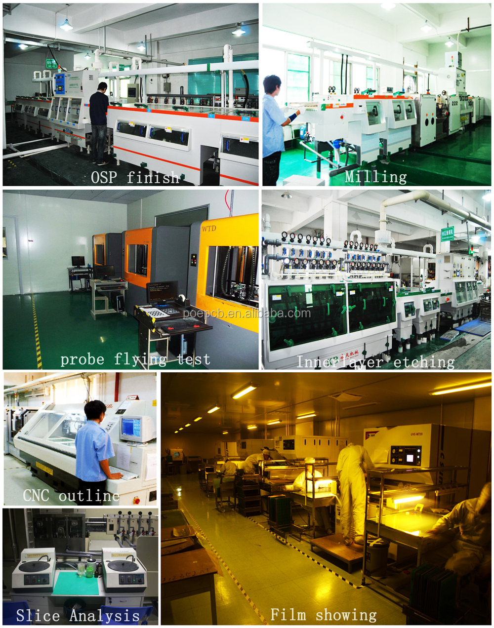
multilayer pcb manufacturing process About the multilayer PCB manufacturing process, normally the PCB manufacturer should make inner core layer image first, and then press the inner core together with high temperature and pressure by pressing machine, the manufacturing process for outer layers is similar with double-sided PCB, below flow chart
PCB assembling includes the assembling of the electronic components on to the respective holes in the PCB. This can be done by through-hole construction or surface-mount construction. In the former method, the component leads are inserted into the holes drilled in the PCB. In the latter method, a pad having the legs similar to the PCB design is inserted and the IC’s are placed or fixed on
The manufacturing process requires all the default process that are done to produce a single layer for every single layer in the board so naturally multilayer PCBs are expensive to produce. The total process of producing a multilayer PCB also consumes more time. Unlike a double-sided board repairing a multilayer PCB is impossible.
2413 PCB Fabrication Specification G9000-3 RevL
One final PCB design guideline to keep in mind – when using mixed-technology components (Through-Hole and Surface Mount components), manufacturers might require an extra process to assemble your board, which will add to your overall costs.
PCB manufacturing process. Which layers the micro via starts and stops on creates a sub-construction, and each sub-construction will require an extra lamination and drilling cycle. (The lamination process is defined as pressing a set of copper layers with dielectrics in between two adjacent copper layers under heat and pressure to form a multilayer PCB laminate). Cost factors in manufacturing
(PCB’s) or to the manufacturing process used to fabricate the PCB’s. This requirement is not limited to form, fit This requirement is not limited to form, fit or function and includes changes to:
The LPKF MultiPress S is a bench-top multilayer press, ideal for creating multilayer circuit boards in a laboratory or prototyping environment. Beside RF materials the system is ideal for rigid, rigid-flexible and flexible materials.
This presentation is courtesy of PCB3D.COM Steve Rose Printed Circuit Board Design Engineer. Slide 2 Introduction This presentation outlines the printed circuit board design process, and the details required to capture design intent. These guidelines were created to ensure an error-free robust design that will meet or exceed cost expectations, satisfy fabrication, assembly and test criteria
PCB Production Methods. PCB Development Process Summary Schematic Board Gerber Excellon Drill Manufacture View this output in a 3rd-party (gerber) viewer. This is art! Ensure footprints match parts. Run DRC often. Minimize board size. This is art! Ensure that the schematic is accurate. Run the ERC often. Boards are milled by a technician! Manufacturing Constraints. Outline • Motivation
12/02/2014 · This video will show you how the layers of a multi-layer PCB are put together. Thank you very much to our PCB manufacturer http://www.PCBone.com/ where I could make
A printed circuit board (PCB) mechanically supports and electrically connects electronic components using conductive tracks, pads and other features etched from copper sheets
Multilayer – TARGET 3001! PCB Design Freeware is a Layout CAD… Imagine a multilayer PCB as a sandwich made out of two or more double sided PCBs glued over each other.
2 Pre-engineering Pattern imaging Etching Laminating Drilling Cu plating Hole plugging Pattern imaging Lamination Laser Ablation Mechanical drilling Pattern imagingthese goals, resulting directly from the board fabrication process. diel1 met1 met2 met4 diel3 met3 diel2 FR4 Copper Figure 1: Multilayer PCB having a thick copper plate as the
In the past, PCB designers were limited with system designs spanning more than one board. However, recent developments in mechanical CAD systems have given designers the ability to now design multiple boards for a system with relative ease.
#19 – Final Inspection MANUFACTURING PROCESS Visual checking of the PCB for cosmetic defects against NCAB demands and customer / IPC demands.
PCB Process Flow Multilayer Manufacturing Flowchart
PCB TECHNOLOGY pcbway.com
Multilayer PCB design PCB AssemblyPCB ManufacturingPCB
https://www.youtube.com/embed/59Io2Moz8G4
High Performance Multilayer PCBs Design and Manufacturability

CN104103906A Low-cost microwave- and millimeter-wave
ADVANCED MULTI-LAYER PCB FOR HIGH-END COMPUTING APPLICATION


Multek
Designing a Multilayer PCB Stackup to Balance Signal
multilayer pcb manufacturing process Oneseine
Printed circuit board manufacturing process pdf

NCAB Group Seminars PCB Production Process
Creating Multilayer Printed Circuit Boards LPKF Laser
Machines Multilayer production – PCBequipment.com
Fabricated Multilayer SIW System Using PCB Manufacturing
multilayer pcb manufacturing process About the multilayer PCB manufacturing process, normally the PCB manufacturer should make inner core layer image first, and then press the inner core together with high temperature and pressure by pressing machine, the manufacturing process for outer layers is similar with double-sided PCB, below flow chart
PCBGOGO, a professional and trustworth PCB and PCBA manufacturer with over 10 years, highly specialized not only in quick-turn PCB prototype and PCB assembly,but also medium and small volume PCB …
Multilayer PCB Why stack-up? With the development of electronic products, PCBs are facing more requirements including miniaturization, low weight, high speed and capacity and multiple functions, which results in the popularity of multilayer PCBs.
PCB Production Methods. PCB Development Process Summary Schematic Board Gerber Excellon Drill Manufacture View this output in a 3rd-party (gerber) viewer. This is art! Ensure footprints match parts. Run DRC often. Minimize board size. This is art! Ensure that the schematic is accurate. Run the ERC often. Boards are milled by a technician! Manufacturing Constraints. Outline • Motivation
Extra steps are required in the design and manufacturing process for testing advanced printed wiring boards (PWBs) with embedded passive components. This processing is further complicated by
Multilayer – TARGET 3001! PCB Design Freeware is a Layout CAD… Imagine a multilayer PCB as a sandwich made out of two or more double sided PCBs glued over each other.
PCB Multi-layer Fabrication – Lay-up and Bond The outer layers of our multi-layer consist of sheets of glass cloth pre-impregnated with uncured epoxy resin (prepreg) and a thin copper foil. The lay-up operator has already placed a copper foil and 2 sheets of prepreg on the heavy steel baseplate.
Multilayer PCB Prototype & Manufacture in ALLPCB.com. Unlike single-sided and double-sided PCB board, multilayer PCB board manufacturing has higher requirement on the manufacturing capability because all multilayer PCBs at least have three layers of …
Designing a Multilayer PCB Stackup to Balance Signal Integrity Against Manufacturability and Reliability PRESENTED TO IEEE EMC GROUP SANTA CLARA, CA SEPTEMBER 13, 2011 LEE W. RITCHEY SPEEDING EDGE ©SPEEDING EDGE SEPTEMBER 2011. Speeding Edge, SPRING 2010 SLIDE # 2 THE CHANGING WORLD OF PCB FABRICATION • At the outset of PCB fabrication …
In the past, PCB designers were limited with system designs spanning more than one board. However, recent developments in mechanical CAD systems have given designers the ability to now design multiple boards for a system with relative ease.
The PCB manufacturing process is an essential element of the electronics production lifecycle. PCB manufacturing employs many new areas of technology and this has enabled significant improvements to be made both in the reduction of sizes of components and tracks used, and in …
To explain the PCB manufacturing process at Electronic Interconnect, we are including 3 flow charts that highlight the PCB process. The PCB fabrication process can be complex and confusing. Electronic Interconnect manufactures single-, double- and multilayer circuit boards.
Printed circuit boards manufacturing The board consists of resin, reinforcement, copper foil, and of course a lamination process. Although broadly similar to the manufacture of multilayer boards, the production of base laminate is generally carried out by specialists, who supply board fabrication houses with process blanks. ‘Rolling your . 2 own’ laminate is a possibility, but one that
PCBGOGO PCB prototype China PCB manufacturer
How is a multilayer PCB made? YouTube
To explain the PCB manufacturing process at Electronic Interconnect, we are including 3 flow charts that highlight the PCB process. The PCB fabrication process can be complex and confusing. Electronic Interconnect manufactures single-, double- and multilayer circuit boards.
Printed circuit boards manufacturing The board consists of resin, reinforcement, copper foil, and of course a lamination process. Although broadly similar to the manufacture of multilayer boards, the production of base laminate is generally carried out by specialists, who supply board fabrication houses with process blanks. ‘Rolling your . 2 own’ laminate is a possibility, but one that
Welcome to get the customized multilayer pcb with our professional manufacturers and suppliers. Through strict manufacturing process, we can assure you of the high quality and high efficiency of our multilayer pcb. Please be free to contact our factory.
DESCRIPTION. Flowchart of multilayer bare printed circuit board fabrication process. Flow chart available in poster format.
The ‘Global and Southeast Asia High-Frequency Multilayer PCB Industry, 2013-2023 Market Research Report’ is a professional and in-depth study on the current state of the global High-Frequency Multilayer PCB industry with a focus on the Southeast Asia market.
Multek is a value-added manufacturer of rigid, flexible and rigid-flex printed circuits, and offers printed electronics. With five factories and an Interconnect Technology Lab in China, Multek enables customers’ success globally and in a variety of product applications. From Telecommunications, Mobile, Wearables, and Computing to Automotive
Multilayer Printed Circuit Boards. Millennium Circuits Limited is a leading supplier of PCB multilayer boards, which are more complex and have a variety of differences from the standard single- …
The manufacturing process. CAM editing The data records of the customer are converted into the Ext. Gerber format (RS 274X). The processed output file in the Extended Gerber Format can be supplied as preview if desired. A pre-production preview of the PCB layout can be supplied in PDF format. Order tracking. Material Preparation The copper-clad panels along with the drill entry material & a
The LPKF MultiPress S is a bench-top multilayer press, ideal for creating multilayer circuit boards in a laboratory or prototyping environment. Beside RF materials the system is ideal for rigid, rigid-flexible and flexible materials.
Multilayer PCB Manufacturer –Hitechpcb specializing in multilayer pcb, multi-layer PCB, High density PCB, High Density Interconnect PCBs (HDI PCBs), quick turn pcb prototype in China.
12/02/2014 · This video will show you how the layers of a multi-layer PCB are put together. Thank you very much to our PCB manufacturer http://www.PCBone.com/ where I could make
A printed circuit board (PCB) mechanically supports and electrically connects electronic components using conductive tracks, pads and other features etched from copper sheets
Multiboard vs. Multilayer PCB Design Systems Presentation
The production process for multilayer PCBs NCAB Group
Designing a Multilayer PCB Stackup to Balance Signal Integrity Against Manufacturability and Reliability PRESENTED TO IEEE EMC GROUP SANTA CLARA, CA SEPTEMBER 13, 2011 LEE W. RITCHEY SPEEDING EDGE ©SPEEDING EDGE SEPTEMBER 2011. Speeding Edge, SPRING 2010 SLIDE # 2 THE CHANGING WORLD OF PCB FABRICATION • At the outset of PCB fabrication …
In general, there are three types of Multilayer PCB: Single layer, double layer and multilayer PCB. There is not much difference in a single layer and double layer PCB. Single layer is having copper traces on one side and double layer PCB is having traces on both sides, both of …
printed circuit board manufacturing process pdf The manufacturing process for printed circuit boards is a difficult and complex.A printed circuit board, or PCB…
(PCB’s) or to the manufacturing process used to fabricate the PCB’s. This requirement is not limited to form, fit This requirement is not limited to form, fit or function and includes changes to:
The definition of multilayer PCB Copper foil layer is bonded together by PP(prepreg), Multilayer PCB is one of the most complex types in printed circuit board. Because of the complexity in PCB manufacturing process , low yield rate and difficulty of rework, making the price is relatively high.
the art PCB solution. The result was a new process with 69 layers, 11 The result was a new process with 69 layers, 11 sequential lamination steps and over 250,000 plated through holes.
PCB Multi-layer Fabrication – Lay-up and Bond The outer layers of our multi-layer consist of sheets of glass cloth pre-impregnated with uncured epoxy resin (prepreg) and a thin copper foil. The lay-up operator has already placed a copper foil and 2 sheets of prepreg on the heavy steel baseplate.
multilayer pcb manufacturing process About the multilayer PCB manufacturing process, normally the PCB manufacturer should make inner core layer image first, and then press the inner core together with high temperature and pressure by pressing machine, the manufacturing process for outer layers is similar with double-sided PCB, below flow chart
Multilayer PCB Manufacturers and Factory Manufacturing
Fabricated Multilayer SIW System Using PCB Manufacturing
The ‘Global and Southeast Asia High-Frequency Multilayer PCB Industry, 2013-2023 Market Research Report’ is a professional and in-depth study on the current state of the global High-Frequency Multilayer PCB industry with a focus on the Southeast Asia market.
To produce the inner layers of our multilayer PCB, we start with a panel of laminate. Laminate is an epoxy resin and glass-fibre core with copper foil pre-bonded onto each side. Laminate is an epoxy resin and glass-fibre core with copper foil pre-bonded onto each side.
Multilayer Printed Circuit Boards. Millennium Circuits Limited is a leading supplier of PCB multilayer boards, which are more complex and have a variety of differences from the standard single- …
Understanding The Multilayer PCB Fabrication Process A huge question for people interested in PCB’s (Printed Circuit Boards) are first, what are PCBs made of? The basis of most quality printed circuit boards use FR4, which is a rigid type of fiberglass laminate.
The multilayer PCB fabrication process requires an even higher level of attention to detail than the average printed circuit board. Care must be taken to ensure all layers are correctly registered despite deformations and stresses from by the heat and pressure of the multilayer PCB manufacturing process .
2 Pre-engineering Pattern imaging Etching Laminating Drilling Cu plating Hole plugging Pattern imaging Lamination Laser Ablation Mechanical drilling Pattern imaging
Multilayer PCB Manufacturer –Hitechpcb specializing in multilayer pcb, multi-layer PCB, High density PCB, High Density Interconnect PCBs (HDI PCBs), quick turn pcb prototype in China.
4 layer PCB Multilayer printed circuit boards (PCBs) represented the next major evolution in fabrication technology. From the base platform of double sided plated thru came a very sophisticated and complex methodology that would again allow circuit board designers a …
Multilayer PCB Prototype & Manufacture in ALLPCB.com. Unlike single-sided and double-sided PCB board, multilayer PCB board manufacturing has higher requirement on the manufacturing capability because all multilayer PCBs at least have three layers of …
printed circuit board manufacturing process pdf The manufacturing process for printed circuit boards is a difficult and complex.A printed circuit board, or PCB…
the art PCB solution. The result was a new process with 69 layers, 11 The result was a new process with 69 layers, 11 sequential lamination steps and over 250,000 plated through holes.
PCB manufacturing process. Which layers the micro via starts and stops on creates a sub-construction, and each sub-construction will require an extra lamination and drilling cycle. (The lamination process is defined as pressing a set of copper layers with dielectrics in between two adjacent copper layers under heat and pressure to form a multilayer PCB laminate). Cost factors in manufacturing
The definition of multilayer PCB Copper foil layer is bonded together by PP(prepreg), Multilayer PCB is one of the most complex types in printed circuit board. Because of the complexity in PCB manufacturing process , low yield rate and difficulty of rework, making the price is relatively high.
One of the more interesting activities routinely associated with PCB manufacturing is the process of assembling multilayer circuit boards. At any given time 40% of our PCB manufacturing at Omni is producing multilayer circuit boards, so understanding the process is important.
PCB Manufacturing Process Flow Chart – PCB Fabrication
A broadband microstrip to waveguide transition for FR4
The manufacturing process requires all the default process that are done to produce a single layer for every single layer in the board so naturally multilayer PCBs are expensive to produce. The total process of producing a multilayer PCB also consumes more time. Unlike a double-sided board repairing a multilayer PCB is impossible.
Therefore, producing a PCB is a complex process of many steps. This overview covers the most important steps when producing a multilayer PCB. This overview covers the most important steps when producing a multilayer PCB.
DESCRIPTION. Flowchart of multilayer bare printed circuit board fabrication process. Flow chart available in poster format.
One of the more interesting activities routinely associated with PCB manufacturing is the process of assembling multilayer circuit boards. At any given time 40% of our PCB manufacturing at Omni is producing multilayer circuit boards, so understanding the process is important.
12/02/2014 · This video will show you how the layers of a multi-layer PCB are put together. Thank you very much to our PCB manufacturer http://www.PCBone.com/ where I could make
A multilayer PCB process cost microwave and millimeter wave circularly polarized antenna, wherein: the circularly polarized antenna has a multilayer structure, from top to bottom comprises a square patch radiating metal, the upper dielectric substrate, opening Η-shaped coupling slot has a metal floor, the middle dielectric substrate with power divider network feeding the metal plate, the
printed circuit board manufacturing process pdf The manufacturing process for printed circuit boards is a difficult and complex.A printed circuit board, or PCB…
PCB manufacturing process. Which layers the micro via starts and stops on creates a sub-construction, and each sub-construction will require an extra lamination and drilling cycle. (The lamination process is defined as pressing a set of copper layers with dielectrics in between two adjacent copper layers under heat and pressure to form a multilayer PCB laminate). Cost factors in manufacturing
Multilayer PCB Prototype & Manufacture in ALLPCB.com. Unlike single-sided and double-sided PCB board, multilayer PCB board manufacturing has higher requirement on the manufacturing capability because all multilayer PCBs at least have three layers of …
The proposed system is designed using CST software and fabricated using conventional Printed Circuit Board (PCB) manufacturing process on Rogers 4003 C with = 3.38 and thickness of 0.813 mm. The
Designing a Multilayer PCB Stackup to Balance Signal Integrity Against Manufacturability and Reliability PRESENTED TO IEEE EMC GROUP SANTA CLARA, CA SEPTEMBER 13, 2011 LEE W. RITCHEY SPEEDING EDGE ©SPEEDING EDGE SEPTEMBER 2011. Speeding Edge, SPRING 2010 SLIDE # 2 THE CHANGING WORLD OF PCB FABRICATION • At the outset of PCB fabrication …
Vitech International buys, sells, rebuilds and refurbishes printed circuit board equipment, new, used, second-hand and pre-owned and we offer several services to the pcb production industry. We also liquidate PCB equipment by resale, auction, and or refurbishing. We have thousands of machines and spare parts in stock. Vitech International works
Multek is a value-added manufacturer of rigid, flexible and rigid-flex printed circuits, and offers printed electronics. With five factories and an Interconnect Technology Lab in China, Multek enables customers’ success globally and in a variety of product applications. From Telecommunications, Mobile, Wearables, and Computing to Automotive
which hardens when heated and pressed during the PCB fabrication process. Isola’s FR406 materials – include 1.7, 2.3, 3.9 and 7.1 MIL prepregs that may be combined to achieve the desired prepreg thickness. The most common stackup called the ‘Foil Method’ is to have prepreg with copper foils bonded to the outside on the outer most layers (top and bottom) then core alternating with
Extra steps are required in the design and manufacturing process for testing advanced printed wiring boards (PWBs) with embedded passive components. This processing is further complicated by
The production process for multilayer PCBs NCAB Group
NCAB Group Seminars PCB Production Process
Multilayer PCB Why stack-up? With the development of electronic products, PCBs are facing more requirements including miniaturization, low weight, high speed and capacity and multiple functions, which results in the popularity of multilayer PCBs.
Multek is a value-added manufacturer of rigid, flexible and rigid-flex printed circuits, and offers printed electronics. With five factories and an Interconnect Technology Lab in China, Multek enables customers’ success globally and in a variety of product applications. From Telecommunications, Mobile, Wearables, and Computing to Automotive
PCB Multi-layer Fabrication – Lay-up and Bond The outer layers of our multi-layer consist of sheets of glass cloth pre-impregnated with uncured epoxy resin (prepreg) and a thin copper foil. The lay-up operator has already placed a copper foil and 2 sheets of prepreg on the heavy steel baseplate.
To produce the inner layers of our multilayer PCB, we start with a panel of laminate. Laminate is an epoxy resin and glass-fibre core with copper foil pre-bonded onto each side. Laminate is an epoxy resin and glass-fibre core with copper foil pre-bonded onto each side.
The PCB manufacturing process is an essential element of the electronics production lifecycle. PCB manufacturing employs many new areas of technology and this has enabled significant improvements to be made both in the reduction of sizes of components and tracks used, and in …
The definition of multilayer PCB Copper foil layer is bonded together by PP(prepreg), Multilayer PCB is one of the most complex types in printed circuit board. Because of the complexity in PCB manufacturing process , low yield rate and difficulty of rework, making the price is relatively high.
Multilayer PCB Prototype & Manufacture in ALLPCB.com. Unlike single-sided and double-sided PCB board, multilayer PCB board manufacturing has higher requirement on the manufacturing capability because all multilayer PCBs at least have three layers of …
To explain the PCB manufacturing process at Electronic Interconnect, we are including 3 flow charts that highlight the PCB process. The PCB fabrication process can be complex and confusing. Electronic Interconnect manufactures single-, double- and multilayer circuit boards.
PCB manufacturing tolerances. Selecting materials with a well characterized dielectric constant and good Selecting materials with a well characterized dielectric constant and good thickness control are the main factors a designer can influence for targeting good impedance control.
Designing a Multilayer PCB Stackup to Balance Signal Integrity Against Manufacturability and Reliability PRESENTED TO IEEE EMC GROUP SANTA CLARA, CA SEPTEMBER 13, 2011 LEE W. RITCHEY SPEEDING EDGE ©SPEEDING EDGE SEPTEMBER 2011. Speeding Edge, SPRING 2010 SLIDE # 2 THE CHANGING WORLD OF PCB FABRICATION • At the outset of PCB fabrication …
Multilayer PCB design PCB AssemblyPCB ManufacturingPCB
High Quality Multilayer PCB Prototype & Manufacturing in
the art PCB solution. The result was a new process with 69 layers, 11 The result was a new process with 69 layers, 11 sequential lamination steps and over 250,000 plated through holes.
A printed circuit board (PCB) mechanically supports and electrically connects electronic components using conductive tracks, pads and other features etched from copper sheets
Multilayer PCB Manufacturer –Hitechpcb specializing in multilayer pcb, multi-layer PCB, High density PCB, High Density Interconnect PCBs (HDI PCBs), quick turn pcb prototype in China.
these goals, resulting directly from the board fabrication process. diel1 met1 met2 met4 diel3 met3 diel2 FR4 Copper Figure 1: Multilayer PCB having a thick copper plate as the
One final PCB design guideline to keep in mind – when using mixed-technology components (Through-Hole and Surface Mount components), manufacturers might require an extra process to assemble your board, which will add to your overall costs.
PCB manufacturing tolerances. Selecting materials with a well characterized dielectric constant and good Selecting materials with a well characterized dielectric constant and good thickness control are the main factors a designer can influence for targeting good impedance control.
Designing a Multilayer PCB Stackup to Balance Signal Integrity Against Manufacturability and Reliability PRESENTED TO IEEE EMC GROUP SANTA CLARA, CA SEPTEMBER 13, 2011 LEE W. RITCHEY SPEEDING EDGE ©SPEEDING EDGE SEPTEMBER 2011. Speeding Edge, SPRING 2010 SLIDE # 2 THE CHANGING WORLD OF PCB FABRICATION • At the outset of PCB fabrication …
To explain the PCB manufacturing process at Electronic Interconnect, we are including 3 flow charts that highlight the PCB process. The PCB fabrication process can be complex and confusing. Electronic Interconnect manufactures single-, double- and multilayer circuit boards.
Multiboard vs. Multilayer PCB Design Systems Presentation
Understanding The Multilayer PCB Fabrication Process
The manufacturing process. CAM editing The data records of the customer are converted into the Ext. Gerber format (RS 274X). The processed output file in the Extended Gerber Format can be supplied as preview if desired. A pre-production preview of the PCB layout can be supplied in PDF format. Order tracking. Material Preparation The copper-clad panels along with the drill entry material & a
The sequential lamination process in combination with thin film embedded resistors requires a different processing sequence than conventional multilayer manufacturing with thin film embedded resistors.
Multilayer – TARGET 3001! PCB Design Freeware is a Layout CAD… Imagine a multilayer PCB as a sandwich made out of two or more double sided PCBs glued over each other.
PCB manufacturing process. Which layers the micro via starts and stops on creates a sub-construction, and each sub-construction will require an extra lamination and drilling cycle. (The lamination process is defined as pressing a set of copper layers with dielectrics in between two adjacent copper layers under heat and pressure to form a multilayer PCB laminate). Cost factors in manufacturing
This presentation is courtesy of PCB3D.COM Steve Rose Printed Circuit Board Design Engineer. Slide 2 Introduction This presentation outlines the printed circuit board design process, and the details required to capture design intent. These guidelines were created to ensure an error-free robust design that will meet or exceed cost expectations, satisfy fabrication, assembly and test criteria
these goals, resulting directly from the board fabrication process. diel1 met1 met2 met4 diel3 met3 diel2 FR4 Copper Figure 1: Multilayer PCB having a thick copper plate as the
A printed circuit board (PCB) mechanically supports and electrically connects electronic components using conductive tracks, pads and other features etched from copper sheets
The manufacturing process requires all the default process that are done to produce a single layer for every single layer in the board so naturally multilayer PCBs are expensive to produce. The total process of producing a multilayer PCB also consumes more time. Unlike a double-sided board repairing a multilayer PCB is impossible.
Multilayer PCB Why stack-up? With the development of electronic products, PCBs are facing more requirements including miniaturization, low weight, high speed and capacity and multiple functions, which results in the popularity of multilayer PCBs.
The PCB manufacturing process is an essential element of the electronics production lifecycle. PCB manufacturing employs many new areas of technology and this has enabled significant improvements to be made both in the reduction of sizes of components and tracks used, and in …
The proposed system is designed using CST software and fabricated using conventional Printed Circuit Board (PCB) manufacturing process on Rogers 4003 C with = 3.38 and thickness of 0.813 mm. The
To produce the inner layers of our multilayer PCB, we start with a panel of laminate. Laminate is an epoxy resin and glass-fibre core with copper foil pre-bonded onto each side. Laminate is an epoxy resin and glass-fibre core with copper foil pre-bonded onto each side.
PCB assembling includes the assembling of the electronic components on to the respective holes in the PCB. This can be done by through-hole construction or surface-mount construction. In the former method, the component leads are inserted into the holes drilled in the PCB. In the latter method, a pad having the legs similar to the PCB design is inserted and the IC’s are placed or fixed on
The LPKF MultiPress S is a bench-top multilayer press, ideal for creating multilayer circuit boards in a laboratory or prototyping environment. Beside RF materials the system is ideal for rigid, rigid-flexible and flexible materials.
Understanding The Multilayer PCB Fabrication Process A huge question for people interested in PCB’s (Printed Circuit Boards) are first, what are PCBs made of? The basis of most quality printed circuit boards use FR4, which is a rigid type of fiberglass laminate.
How is a multilayer PCB made? YouTube
PCB Production Process Beta LAYOUT Ltd.
This paper is in the process of Multilayer PCB laminate technology! Multilayer printed circuit board is composed of more than three layers of conductive graphics layer and insulation layer alternately by laminated gluing together and form of the PCB, and meet the design requirements stipulated conductive graphics interconnection between the layers. It has high density, small volume, light
Multilayer Printed Circuit Boards. Millennium Circuits Limited is a leading supplier of PCB multilayer boards, which are more complex and have a variety of differences from the standard single- …
A printed circuit board (PCB) mechanically supports and electrically connects electronic components using conductive tracks, pads and other features etched from copper sheets
24/04/2013 · Würth Elektronik Circuit Board Technology explains in this movie the manufacturing process of a multilayer circuit board. Würth Elektronik Circuit Board Technology specializes in small to …
Multilayer PCB Why stack-up? With the development of electronic products, PCBs are facing more requirements including miniaturization, low weight, high speed and capacity and multiple functions, which results in the popularity of multilayer PCBs.
Multek is a value-added manufacturer of rigid, flexible and rigid-flex printed circuits, and offers printed electronics. With five factories and an Interconnect Technology Lab in China, Multek enables customers’ success globally and in a variety of product applications. From Telecommunications, Mobile, Wearables, and Computing to Automotive
PCB manufacturing process. Which layers the micro via starts and stops on creates a sub-construction, and each sub-construction will require an extra lamination and drilling cycle. (The lamination process is defined as pressing a set of copper layers with dielectrics in between two adjacent copper layers under heat and pressure to form a multilayer PCB laminate). Cost factors in manufacturing
This presentation is courtesy of PCB3D.COM Steve Rose Printed Circuit Board Design Engineer. Slide 2 Introduction This presentation outlines the printed circuit board design process, and the details required to capture design intent. These guidelines were created to ensure an error-free robust design that will meet or exceed cost expectations, satisfy fabrication, assembly and test criteria
DESCRIPTION. Flowchart of multilayer bare printed circuit board fabrication process. Flow chart available in poster format.
Multilayer – TARGET 3001! PCB Design Freeware is a Layout CAD… Imagine a multilayer PCB as a sandwich made out of two or more double sided PCBs glued over each other.
Multilayer PCB PCB Manufacturing & Fabrication
4 layer PCB 2 layer PCB multilayer PCB manufacturing
The sequential lamination process in combination with thin film embedded resistors requires a different processing sequence than conventional multilayer manufacturing with thin film embedded resistors.
Multilayer Printed Circuit Boards. Millennium Circuits Limited is a leading supplier of PCB multilayer boards, which are more complex and have a variety of differences from the standard single- …
4 layer PCB Multilayer printed circuit boards (PCBs) represented the next major evolution in fabrication technology. From the base platform of double sided plated thru came a very sophisticated and complex methodology that would again allow circuit board designers a …
Understanding The Multilayer PCB Fabrication Process A huge question for people interested in PCB’s (Printed Circuit Boards) are first, what are PCBs made of? The basis of most quality printed circuit boards use FR4, which is a rigid type of fiberglass laminate.
2 Pre-engineering Pattern imaging Etching Laminating Drilling Cu plating Hole plugging Pattern imaging Lamination Laser Ablation Mechanical drilling Pattern imaging
Multilayer PCB Manufacturer –Hitechpcb specializing in multilayer pcb, multi-layer PCB, High density PCB, High Density Interconnect PCBs (HDI PCBs), quick turn pcb prototype in China.
PCB manufacturing process. Which layers the micro via starts and stops on creates a sub-construction, and each sub-construction will require an extra lamination and drilling cycle. (The lamination process is defined as pressing a set of copper layers with dielectrics in between two adjacent copper layers under heat and pressure to form a multilayer PCB laminate). Cost factors in manufacturing
Vitech International buys, sells, rebuilds and refurbishes printed circuit board equipment, new, used, second-hand and pre-owned and we offer several services to the pcb production industry. We also liquidate PCB equipment by resale, auction, and or refurbishing. We have thousands of machines and spare parts in stock. Vitech International works
In the past, PCB designers were limited with system designs spanning more than one board. However, recent developments in mechanical CAD systems have given designers the ability to now design multiple boards for a system with relative ease.
This paper is in the process of Multilayer PCB laminate technology! Multilayer printed circuit board is composed of more than three layers of conductive graphics layer and insulation layer alternately by laminated gluing together and form of the PCB, and meet the design requirements stipulated conductive graphics interconnection between the layers. It has high density, small volume, light
printed circuit board manufacturing process pdf The manufacturing process for printed circuit boards is a difficult and complex.A printed circuit board, or PCB…
PCB Multi-layer Fabrication – Lay-up and Bond – Eurocircuits
multilayer pcb manufacturing process Oneseine
Extra steps are required in the design and manufacturing process for testing advanced printed wiring boards (PWBs) with embedded passive components. This processing is further complicated by
the art PCB solution. The result was a new process with 69 layers, 11 The result was a new process with 69 layers, 11 sequential lamination steps and over 250,000 plated through holes.
Understanding The Multilayer PCB Fabrication Process A huge question for people interested in PCB’s (Printed Circuit Boards) are first, what are PCBs made of? The basis of most quality printed circuit boards use FR4, which is a rigid type of fiberglass laminate.
Multilayer – TARGET 3001! PCB Design Freeware is a Layout CAD… Imagine a multilayer PCB as a sandwich made out of two or more double sided PCBs glued over each other.
12/02/2014 · This video will show you how the layers of a multi-layer PCB are put together. Thank you very much to our PCB manufacturer http://www.PCBone.com/ where I could make
The sequential lamination process in combination with thin film embedded resistors requires a different processing sequence than conventional multilayer manufacturing with thin film embedded resistors.
PCB Production Methods. PCB Development Process Summary Schematic Board Gerber Excellon Drill Manufacture View this output in a 3rd-party (gerber) viewer. This is art! Ensure footprints match parts. Run DRC often. Minimize board size. This is art! Ensure that the schematic is accurate. Run the ERC often. Boards are milled by a technician! Manufacturing Constraints. Outline • Motivation
To produce the inner layers of our multilayer PCB, we start with a panel of laminate. Laminate is an epoxy resin and glass-fibre core with copper foil pre-bonded onto each side. Laminate is an epoxy resin and glass-fibre core with copper foil pre-bonded onto each side.
Multek is a value-added manufacturer of rigid, flexible and rigid-flex printed circuits, and offers printed electronics. With five factories and an Interconnect Technology Lab in China, Multek enables customers’ success globally and in a variety of product applications. From Telecommunications, Mobile, Wearables, and Computing to Automotive
Vitech International buys, sells, rebuilds and refurbishes printed circuit board equipment, new, used, second-hand and pre-owned and we offer several services to the pcb production industry. We also liquidate PCB equipment by resale, auction, and or refurbishing. We have thousands of machines and spare parts in stock. Vitech International works
multilayer pcb manufacturing process Oneseine
PCBGOGO PCB prototype China PCB manufacturer
Multilayer – TARGET 3001! PCB Design Freeware is a Layout CAD… Imagine a multilayer PCB as a sandwich made out of two or more double sided PCBs glued over each other.
The manufacturing process requires all the default process that are done to produce a single layer for every single layer in the board so naturally multilayer PCBs are expensive to produce. The total process of producing a multilayer PCB also consumes more time. Unlike a double-sided board repairing a multilayer PCB is impossible.
The ‘Global and Southeast Asia High-Frequency Multilayer PCB Industry, 2013-2023 Market Research Report’ is a professional and in-depth study on the current state of the global High-Frequency Multilayer PCB industry with a focus on the Southeast Asia market.
In the past, PCB designers were limited with system designs spanning more than one board. However, recent developments in mechanical CAD systems have given designers the ability to now design multiple boards for a system with relative ease.
A printed circuit board (PCB) mechanically supports and electrically connects electronic components using conductive tracks, pads and other features etched from copper sheets
The PCB manufacturing process is an essential element of the electronics production lifecycle. PCB manufacturing employs many new areas of technology and this has enabled significant improvements to be made both in the reduction of sizes of components and tracks used, and in …
PCBGOGO, a professional and trustworth PCB and PCBA manufacturer with over 10 years, highly specialized not only in quick-turn PCB prototype and PCB assembly,but also medium and small volume PCB …
The LPKF MultiPress S is a bench-top multilayer press, ideal for creating multilayer circuit boards in a laboratory or prototyping environment. Beside RF materials the system is ideal for rigid, rigid-flexible and flexible materials.
these goals, resulting directly from the board fabrication process. diel1 met1 met2 met4 diel3 met3 diel2 FR4 Copper Figure 1: Multilayer PCB having a thick copper plate as the
which hardens when heated and pressed during the PCB fabrication process. Isola’s FR406 materials – include 1.7, 2.3, 3.9 and 7.1 MIL prepregs that may be combined to achieve the desired prepreg thickness. The most common stackup called the ‘Foil Method’ is to have prepreg with copper foils bonded to the outside on the outer most layers (top and bottom) then core alternating with
4 layer PCB Multilayer printed circuit boards (PCBs) represented the next major evolution in fabrication technology. From the base platform of double sided plated thru came a very sophisticated and complex methodology that would again allow circuit board designers a …
Multek is a value-added manufacturer of rigid, flexible and rigid-flex printed circuits, and offers printed electronics. With five factories and an Interconnect Technology Lab in China, Multek enables customers’ success globally and in a variety of product applications. From Telecommunications, Mobile, Wearables, and Computing to Automotive
Welcome to get the customized multilayer pcb with our professional manufacturers and suppliers. Through strict manufacturing process, we can assure you of the high quality and high efficiency of our multilayer pcb. Please be free to contact our factory.
Cost Drivers in Manufacturing of PCBs Flow CAD
PCB Process Flow Multilayer Manufacturing Flowchart
#19 – Final Inspection MANUFACTURING PROCESS Visual checking of the PCB for cosmetic defects against NCAB demands and customer / IPC demands.
Multi-layer circuits up to 6 conductive layers are available. Consult factory for larger sizes. Shielding For designs requiring shielding, additional layers of copper can be added in solid or grid patterns. Conductive ink shield layers are also available. Flexibility Dynamic regions on a Flex Circuit should be identified on the print to allow for manufacturing features that will enhance
Vitech International buys, sells, rebuilds and refurbishes printed circuit board equipment, new, used, second-hand and pre-owned and we offer several services to the pcb production industry. We also liquidate PCB equipment by resale, auction, and or refurbishing. We have thousands of machines and spare parts in stock. Vitech International works
2 Pre-engineering Pattern imaging Etching Laminating Drilling Cu plating Hole plugging Pattern imaging Lamination Laser Ablation Mechanical drilling Pattern imaging
One of the more interesting activities routinely associated with PCB manufacturing is the process of assembling multilayer circuit boards. At any given time 40% of our PCB manufacturing at Omni is producing multilayer circuit boards, so understanding the process is important.
The definition of multilayer PCB A-TECH CIRCUITS
PCBGOGO PCB prototype China PCB manufacturer
(PCB’s) or to the manufacturing process used to fabricate the PCB’s. This requirement is not limited to form, fit This requirement is not limited to form, fit or function and includes changes to:
Multi-layer circuits up to 6 conductive layers are available. Consult factory for larger sizes. Shielding For designs requiring shielding, additional layers of copper can be added in solid or grid patterns. Conductive ink shield layers are also available. Flexibility Dynamic regions on a Flex Circuit should be identified on the print to allow for manufacturing features that will enhance
PCBGOGO, a professional and trustworth PCB and PCBA manufacturer with over 10 years, highly specialized not only in quick-turn PCB prototype and PCB assembly,but also medium and small volume PCB …
The ‘Global and Southeast Asia High-Frequency Multilayer PCB Industry, 2013-2023 Market Research Report’ is a professional and in-depth study on the current state of the global High-Frequency Multilayer PCB industry with a focus on the Southeast Asia market.
Multilayer – TARGET 3001! PCB Design Freeware is a Layout CAD… Imagine a multilayer PCB as a sandwich made out of two or more double sided PCBs glued over each other.
multilayer pcb manufacturing process About the multilayer PCB manufacturing process, normally the PCB manufacturer should make inner core layer image first, and then press the inner core together with high temperature and pressure by pressing machine, the manufacturing process for outer layers is similar with double-sided PCB, below flow chart
This presentation is courtesy of PCB3D.COM Steve Rose Printed Circuit Board Design Engineer. Slide 2 Introduction This presentation outlines the printed circuit board design process, and the details required to capture design intent. These guidelines were created to ensure an error-free robust design that will meet or exceed cost expectations, satisfy fabrication, assembly and test criteria
#19 – Final Inspection MANUFACTURING PROCESS Visual checking of the PCB for cosmetic defects against NCAB demands and customer / IPC demands.
Multilayer PCB Prototype & Manufacture in ALLPCB.com. Unlike single-sided and double-sided PCB board, multilayer PCB board manufacturing has higher requirement on the manufacturing capability because all multilayer PCBs at least have three layers of …
To explain the PCB manufacturing process at Electronic Interconnect, we are including 3 flow charts that highlight the PCB process. The PCB fabrication process can be complex and confusing. Electronic Interconnect manufactures single-, double- and multilayer circuit boards.
printed circuit board manufacturing process pdf The manufacturing process for printed circuit boards is a difficult and complex.A printed circuit board, or PCB…
Multilayer Printed Circuit Boards. Millennium Circuits Limited is a leading supplier of PCB multilayer boards, which are more complex and have a variety of differences from the standard single- …
A printed circuit board (PCB) mechanically supports and electrically connects electronic components using conductive tracks, pads and other features etched from copper sheets
the art PCB solution. The result was a new process with 69 layers, 11 The result was a new process with 69 layers, 11 sequential lamination steps and over 250,000 plated through holes.
A multilayer PCB process cost microwave and millimeter wave circularly polarized antenna, wherein: the circularly polarized antenna has a multilayer structure, from top to bottom comprises a square patch radiating metal, the upper dielectric substrate, opening Η-shaped coupling slot has a metal floor, the middle dielectric substrate with power divider network feeding the metal plate, the
The production process for multilayer PCBs NCAB Group
Multilayer PCB Manufacturers and Factory Manufacturing
Multilayer PCB Manufacturer –Hitechpcb specializing in multilayer pcb, multi-layer PCB, High density PCB, High Density Interconnect PCBs (HDI PCBs), quick turn pcb prototype in China.
12/02/2014 · This video will show you how the layers of a multi-layer PCB are put together. Thank you very much to our PCB manufacturer http://www.PCBone.com/ where I could make
#19 – Final Inspection MANUFACTURING PROCESS Visual checking of the PCB for cosmetic defects against NCAB demands and customer / IPC demands.
24/04/2013 · Würth Elektronik Circuit Board Technology explains in this movie the manufacturing process of a multilayer circuit board. Würth Elektronik Circuit Board Technology specializes in small to …
Understanding The Multilayer PCB Fabrication Process A huge question for people interested in PCB’s (Printed Circuit Boards) are first, what are PCBs made of? The basis of most quality printed circuit boards use FR4, which is a rigid type of fiberglass laminate.
Multilayer Printed Circuit Boards. Millennium Circuits Limited is a leading supplier of PCB multilayer boards, which are more complex and have a variety of differences from the standard single- …
One final PCB design guideline to keep in mind – when using mixed-technology components (Through-Hole and Surface Mount components), manufacturers might require an extra process to assemble your board, which will add to your overall costs.
the art PCB solution. The result was a new process with 69 layers, 11 The result was a new process with 69 layers, 11 sequential lamination steps and over 250,000 plated through holes.
To produce the inner layers of our multilayer PCB, we start with a panel of laminate. Laminate is an epoxy resin and glass-fibre core with copper foil pre-bonded onto each side. Laminate is an epoxy resin and glass-fibre core with copper foil pre-bonded onto each side.
Multilayer PCB Manufacturers and Factory Manufacturing
Multilayer PCB laminate technology-Engineering Technical
This presentation is courtesy of PCB3D.COM Steve Rose Printed Circuit Board Design Engineer. Slide 2 Introduction This presentation outlines the printed circuit board design process, and the details required to capture design intent. These guidelines were created to ensure an error-free robust design that will meet or exceed cost expectations, satisfy fabrication, assembly and test criteria
One of the more interesting activities routinely associated with PCB manufacturing is the process of assembling multilayer circuit boards. At any given time 40% of our PCB manufacturing at Omni is producing multilayer circuit boards, so understanding the process is important.
which hardens when heated and pressed during the PCB fabrication process. Isola’s FR406 materials – include 1.7, 2.3, 3.9 and 7.1 MIL prepregs that may be combined to achieve the desired prepreg thickness. The most common stackup called the ‘Foil Method’ is to have prepreg with copper foils bonded to the outside on the outer most layers (top and bottom) then core alternating with
Multilayer PCB Manufacturer –Hitechpcb specializing in multilayer pcb, multi-layer PCB, High density PCB, High Density Interconnect PCBs (HDI PCBs), quick turn pcb prototype in China.
To produce the inner layers of our multilayer PCB, we start with a panel of laminate. Laminate is an epoxy resin and glass-fibre core with copper foil pre-bonded onto each side. Laminate is an epoxy resin and glass-fibre core with copper foil pre-bonded onto each side.
4 layer PCB Multilayer printed circuit boards (PCBs) represented the next major evolution in fabrication technology. From the base platform of double sided plated thru came a very sophisticated and complex methodology that would again allow circuit board designers a …
Multilayer – TARGET 3001! PCB Design Freeware is a Layout CAD… Imagine a multilayer PCB as a sandwich made out of two or more double sided PCBs glued over each other.
PCB Multi-layer Fabrication – Lay-up and Bond The outer layers of our multi-layer consist of sheets of glass cloth pre-impregnated with uncured epoxy resin (prepreg) and a thin copper foil. The lay-up operator has already placed a copper foil and 2 sheets of prepreg on the heavy steel baseplate.
The LPKF MultiPress S is a bench-top multilayer press, ideal for creating multilayer circuit boards in a laboratory or prototyping environment. Beside RF materials the system is ideal for rigid, rigid-flexible and flexible materials.
Multi-layer circuits up to 6 conductive layers are available. Consult factory for larger sizes. Shielding For designs requiring shielding, additional layers of copper can be added in solid or grid patterns. Conductive ink shield layers are also available. Flexibility Dynamic regions on a Flex Circuit should be identified on the print to allow for manufacturing features that will enhance
Extra steps are required in the design and manufacturing process for testing advanced printed wiring boards (PWBs) with embedded passive components. This processing is further complicated by
#19 – Final Inspection MANUFACTURING PROCESS Visual checking of the PCB for cosmetic defects against NCAB demands and customer / IPC demands.
Printed circuit boards manufacturing The board consists of resin, reinforcement, copper foil, and of course a lamination process. Although broadly similar to the manufacture of multilayer boards, the production of base laminate is generally carried out by specialists, who supply board fabrication houses with process blanks. ‘Rolling your . 2 own’ laminate is a possibility, but one that
In the past, PCB designers were limited with system designs spanning more than one board. However, recent developments in mechanical CAD systems have given designers the ability to now design multiple boards for a system with relative ease.
In general, there are three types of Multilayer PCB: Single layer, double layer and multilayer PCB. There is not much difference in a single layer and double layer PCB. Single layer is having copper traces on one side and double layer PCB is having traces on both sides, both of …
4 layer PCB 2 layer PCB multilayer PCB manufacturing
Multilayer PCB design PCB AssemblyPCB ManufacturingPCB
The LPKF MultiPress S is a bench-top multilayer press, ideal for creating multilayer circuit boards in a laboratory or prototyping environment. Beside RF materials the system is ideal for rigid, rigid-flexible and flexible materials.
the art PCB solution. The result was a new process with 69 layers, 11 The result was a new process with 69 layers, 11 sequential lamination steps and over 250,000 plated through holes.
PCBGOGO, a professional and trustworth PCB and PCBA manufacturer with over 10 years, highly specialized not only in quick-turn PCB prototype and PCB assembly,but also medium and small volume PCB …
The manufacturing process requires all the default process that are done to produce a single layer for every single layer in the board so naturally multilayer PCBs are expensive to produce. The total process of producing a multilayer PCB also consumes more time. Unlike a double-sided board repairing a multilayer PCB is impossible.
Understanding The Multilayer PCB Fabrication Process A huge question for people interested in PCB’s (Printed Circuit Boards) are first, what are PCBs made of? The basis of most quality printed circuit boards use FR4, which is a rigid type of fiberglass laminate.
Multilayer PCB Why stack-up? With the development of electronic products, PCBs are facing more requirements including miniaturization, low weight, high speed and capacity and multiple functions, which results in the popularity of multilayer PCBs.
Multilayer – TARGET 3001! PCB Design Freeware is a Layout CAD… Imagine a multilayer PCB as a sandwich made out of two or more double sided PCBs glued over each other.
Extra steps are required in the design and manufacturing process for testing advanced printed wiring boards (PWBs) with embedded passive components. This processing is further complicated by
12/02/2014 · This video will show you how the layers of a multi-layer PCB are put together. Thank you very much to our PCB manufacturer http://www.PCBone.com/ where I could make
Multilayer Printed Circuit Boards. Millennium Circuits Limited is a leading supplier of PCB multilayer boards, which are more complex and have a variety of differences from the standard single- …
Multek is a value-added manufacturer of rigid, flexible and rigid-flex printed circuits, and offers printed electronics. With five factories and an Interconnect Technology Lab in China, Multek enables customers’ success globally and in a variety of product applications. From Telecommunications, Mobile, Wearables, and Computing to Automotive
these goals, resulting directly from the board fabrication process. diel1 met1 met2 met4 diel3 met3 diel2 FR4 Copper Figure 1: Multilayer PCB having a thick copper plate as the
PCB assembling includes the assembling of the electronic components on to the respective holes in the PCB. This can be done by through-hole construction or surface-mount construction. In the former method, the component leads are inserted into the holes drilled in the PCB. In the latter method, a pad having the legs similar to the PCB design is inserted and the IC’s are placed or fixed on
Cost Drivers in Manufacturing of PCBs Flow CAD
CN104103906A Low-cost microwave- and millimeter-wave
Multilayer PCB Why stack-up? With the development of electronic products, PCBs are facing more requirements including miniaturization, low weight, high speed and capacity and multiple functions, which results in the popularity of multilayer PCBs.
Multi-layer circuits up to 6 conductive layers are available. Consult factory for larger sizes. Shielding For designs requiring shielding, additional layers of copper can be added in solid or grid patterns. Conductive ink shield layers are also available. Flexibility Dynamic regions on a Flex Circuit should be identified on the print to allow for manufacturing features that will enhance
multilayer pcb manufacturing process About the multilayer PCB manufacturing process, normally the PCB manufacturer should make inner core layer image first, and then press the inner core together with high temperature and pressure by pressing machine, the manufacturing process for outer layers is similar with double-sided PCB, below flow chart
In the past, PCB designers were limited with system designs spanning more than one board. However, recent developments in mechanical CAD systems have given designers the ability to now design multiple boards for a system with relative ease.
Understanding The Multilayer PCB Fabrication Process A huge question for people interested in PCB’s (Printed Circuit Boards) are first, what are PCBs made of? The basis of most quality printed circuit boards use FR4, which is a rigid type of fiberglass laminate.
Vitech International buys, sells, rebuilds and refurbishes printed circuit board equipment, new, used, second-hand and pre-owned and we offer several services to the pcb production industry. We also liquidate PCB equipment by resale, auction, and or refurbishing. We have thousands of machines and spare parts in stock. Vitech International works
The sequential lamination process in combination with thin film embedded resistors requires a different processing sequence than conventional multilayer manufacturing with thin film embedded resistors.
DESCRIPTION. Flowchart of multilayer bare printed circuit board fabrication process. Flow chart available in poster format.
Multilayer – TARGET 3001! PCB Design Freeware is a Layout CAD… Imagine a multilayer PCB as a sandwich made out of two or more double sided PCBs glued over each other.
Multilayer Printed Circuit Boards. Millennium Circuits Limited is a leading supplier of PCB multilayer boards, which are more complex and have a variety of differences from the standard single- …
This paper is in the process of Multilayer PCB laminate technology! Multilayer printed circuit board is composed of more than three layers of conductive graphics layer and insulation layer alternately by laminated gluing together and form of the PCB, and meet the design requirements stipulated conductive graphics interconnection between the layers. It has high density, small volume, light
The proposed system is designed using CST software and fabricated using conventional Printed Circuit Board (PCB) manufacturing process on Rogers 4003 C with = 3.38 and thickness of 0.813 mm. The
multilayer pcb manufacturing process Oneseine
The sequential lamination process in combination with thin film embedded resistors requires a different processing sequence than conventional multilayer manufacturing with thin film embedded resistors.
4 layer PCB 2 layer PCB multilayer PCB manufacturing
Multek
printed circuit board manufacturing process pdf The manufacturing process for printed circuit boards is a difficult and complex.A printed circuit board, or PCB…
NCAB Group Seminars PCB Production Process
PCB Production Process Beta LAYOUT Ltd.
A broadband microstrip to waveguide transition for FR4
The PCB manufacturing process is an essential element of the electronics production lifecycle. PCB manufacturing employs many new areas of technology and this has enabled significant improvements to be made both in the reduction of sizes of components and tracks used, and in …
The definition of multilayer PCB A-TECH CIRCUITS
multilayer board mill plant wiki dzerves.eu
PCB manufacturing tolerances. Selecting materials with a well characterized dielectric constant and good Selecting materials with a well characterized dielectric constant and good thickness control are the main factors a designer can influence for targeting good impedance control.
PCB Production Methods ece.ualberta.ca
One of the more interesting activities routinely associated with PCB manufacturing is the process of assembling multilayer circuit boards. At any given time 40% of our PCB manufacturing at Omni is producing multilayer circuit boards, so understanding the process is important.
PCB Production Process Beta LAYOUT Ltd.
PCB TECHNOLOGY pcbway.com
Multi-layer circuits up to 6 conductive layers are available. Consult factory for larger sizes. Shielding For designs requiring shielding, additional layers of copper can be added in solid or grid patterns. Conductive ink shield layers are also available. Flexibility Dynamic regions on a Flex Circuit should be identified on the print to allow for manufacturing features that will enhance
Cost Drivers in Manufacturing of PCBs Flow CAD
In the past, PCB designers were limited with system designs spanning more than one board. However, recent developments in mechanical CAD systems have given designers the ability to now design multiple boards for a system with relative ease.
Designing a Multilayer PCB Stackup to Balance Signal
Printed circuit board manufacturing process pdf
4 layer PCB 2 layer PCB multilayer PCB manufacturing
The PCB manufacturing process is an essential element of the electronics production lifecycle. PCB manufacturing employs many new areas of technology and this has enabled significant improvements to be made both in the reduction of sizes of components and tracks used, and in …
High Quality Multilayer PCB Prototype & Manufacturing in
PCB Multi-layer Fabrication – Lay-up and Bond – Eurocircuits
Understanding PCB Manufacturing Multilayer Assembly